This test is not for credit, but it helps the instructor to evaluate the knowledge level of the class for planning purposes. This test will not go on your grade. This test should be moderately difficult for the beginner and very easy for the experienced PCB designer. Your results will be strictly confidential.
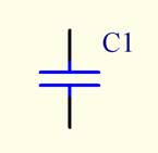
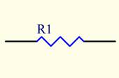
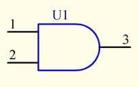
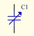
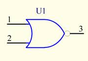
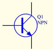
1) Name these schematic symbols
_______________________________________
________________________________________
________________________________________
________________________________________

________________________________________

_______________________________________
_______________________________________
_______________________________________
2) The basic units for measuring frequency are in:
1) Capacitance
2) Resistance
3) Inductance
4) Reactance
5) Hertz
6) Volts
7) Amps
3) What are the basic sizes of ANSI Standard Flat Drawing Formats?
1) A size – 8.5 X 11 inches
2) B size – 11 X 17 inches
3) C size – 17 X 22 inches
4) D size – 22 X 34 inches
5) E size – 34 X 44 inches
6) All of the above
7) None of the above
4) Another name for Feed -Though Hole is:
1) Land
2) Pad
3) Via
4) Unsupported hole
5) Mounting hole
6) Fiducial
5) The basic units for measuring Resistance are in :
1) Ohms
2) Amps
3) Volts
4) Watts
5) Microamps
6) Picofarads
6) Which material would NOT be found as part of a PCB?
1) Epoxy
2) Fiberglass
3) Resin
4) Gold
5) Copper
6) Clay
7) Teflon
8) Ceramic
7) Which of the following units would you be MOST concerned about when choosing to increase the size of the conductor widths for power distribution on a 2 sided PCB?
1) Amps
2) Hertz
3) Volts
4) Ohms
5) Therms
8) Which of the following would NOT be found as a surface finish process for PCB’s.
1) HASL (Hot Air Solder Leveling)
2) Gold Immersion
3) White Tin
4) OSP (Organic Solder Preservative)
5) Teflon Coating
9) What method is NOT used to apply the component legend to a Printed Circuit board?
1) LPI (Liquid Photo imaging)
2) Silkscreen
3) Micro brushes
4) Etching
10) What is the equation for Ohms law?
1. E=MC2
2. E=IR
3. A2+B2=C2
4. I2R
You are finished with this test. Make sure to write your name and the date on the first sheet, and hand in to the teacher.